This project is a simple 32-bit microcontroller written entirely in Logisim from basic logic gates. It's accompanied by an assembler written in Swift. I created this project while studying at UAT (Phoenix, AZ) to gain an understanding of logic operations and CPUs.
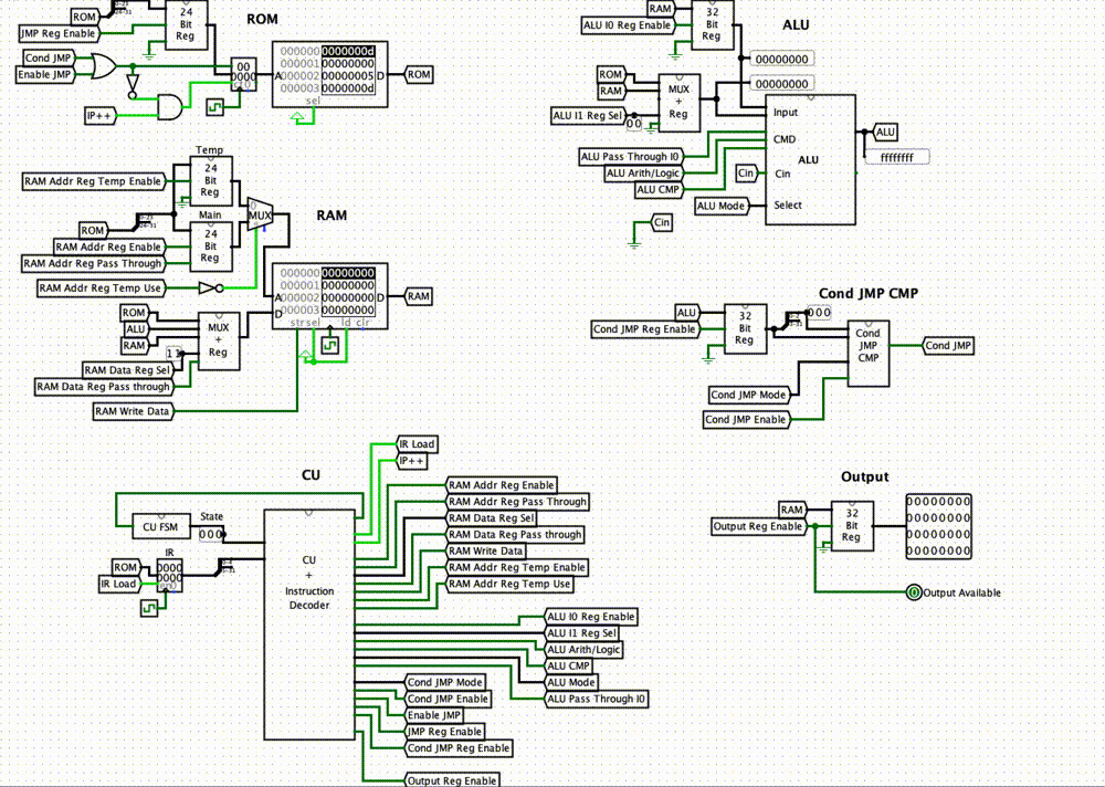
To give a little insight into this project, we could either start the journey with a “written program” and peel away layers of abstraction, or start with “basic logic gates” and explore how it is possible to build a working CPU from these building blocks by increasing the complexity through layers of abstraction. I think both journeys are interesting, and I will start with the former, letting them eventually meet roughly where the overview image above is located.
Before we dive in, I want to note that not everything from this exercise can be directly transferred to modern computers. Modern computer and CPU architectures are so incredibly complicated that it is virtually impossible to understand everything from the transistor layer through all layers of abstraction up to drawing pixels on a screen. But this simplified version is still very helpful in getting an idea of how CPUs and computers roughly do their thing. Another thing worth noting is that the whole thing is technically called a “microcontroller” and the CPU is “just” an important part of it. To get the terminology correct: The mere CPU here is accompanied by RAM, ROM and Output to be actually useful, and such a package is often referred to as a “microcontroller”.
The highest level of abstraction we begin with is assembly code. I know many haven't touched assembly code before, and practically for most applications it's not necessary or even advisable to write assembly code directly. But its goal is very similar to other programming languages like C++, to have a layer of abstraction to avoid writing machine code directly. Machine code is the actual bits and bytes a CPU can understand and work with. To write code in a way that is more relatable to humans, assembly or C++ code needs to be translated into machine code by an assembler or a compiler. Assembly is structurally very similar to machine code, but you don't have to memorize the so-called Opcodes – the actual number you use to tell the CPU to move some data into a register, for example, but instead use an instruction like mov. Since I wanted to have that luxury, I wrote an assembler that can assemble very simple x86 assembly into machine code which the CPU I built here is able to understand. With this, I was in a position to write this simple program for calculating Fibonacci numbers in assembly code…
; Calculate Fibonacci Numbers
SECTION .data
  Fnumber 5   ; number of numbers to produce
  F1 0        ; Initial number 1
  F2 1        ; Initial number 2
  Result 1    ; Variable to store result

SECTION .text
  out F1
  out F2
loop:
  add Result, F1
  mov F1, F2
  mov F2, Result
  out Result
  dec Fnumber
  jnz loop
…and turn it into machine code, which looks like this:
v2.0 raw
d 0 5
d 1 0
d 2 1
d 3 1
1b 1
1b 2
6 3 1
c 1 2
c 2 3
1b 3
18 0
16 10
This is formatted in a way that the ROM component in Logisim can read it. Which brings me back to the overview image. The “ROM” part at the top left is responsible for managing everything directly related to the program code, so the assembled code for calculating the Fibonacci numbers can also be loaded here. The RAM part below is responsible for accessing and storing working data. Further down the part labeled “CU” represents the Control Unit of the CPU. It orchestrates all the other parts to create a working whole. On the right side, the Arithmetic logic unit ALU performs calculations or logic operations on binary numbers, such as addition, multiplication, logical AND as well as comparisons. I've also created a part that implements the logic to perform conditional jumps based on the results of comparisons made by the ALU. This part is called the “Conditional Jump Comparison Unit” Conditions JMP CMP and it gives me the ability to use simple if statements. With instructions like “jump if not equal” and a ROM memory address pointing to end of a code block, that code block is only executed if the two numbers are equal. And finally, the “Output” so we also have a way to look at the results this conglomeration of parts produces.
Let's take a step back and look at the machine code again. The first column is the opcode, basically a number that tells the CPU what instruction to execute. The machine code is written in base 16 or hexadecimal numbers, which conveniently represents a byte (usually eight “bits” or “0s and 1s”) with two hexadecimal digits, hence why you also see some letters. The second and optionally the third column represent operands for the previously defined instruction. For example, the inc instruction needs only one operand, which is the address of the number to be incremented by one. The mov instruction, on the other hand, requires two operands – where to “move” or stored something and what that something is or where it comes from.
To be able to execute all these instructions, we need quite a bit of functionality and logic, just to name a few: We need an Instruction Pointer (IP), which is a register that points to the address of the instruction currently being executed, we need a way to access data in ROM and RAM, additionally write to the RAM and move data between various parts, we need a way to fetch, decode and execute instructions and operands and do so in the right order, and we need a way to actually do something useful with the data like performing calculations…
Okay, let's not get ahead of ourselves! Let us zoom all the way in and have a look at the simplest logic building blocks and work our way up – To be honest, we're not “zoomed all the way in”, we're ignoring the layers of transistors, silicon, quantum… tin order not to unnecessarily complicate what we want to focus on here. Here we have logic gates such as AND, OR, NAND… The simplest versions of those take two inputs and according to their logic function, output one bit. For example AND will output a 1 if the first AND the second input are both 1. For all other input combinations the output will be 0. For the NAND (Not AND) version the output is inverted, which mans that if an AND gate would output a 1, a NAND would output a 0 and vice versa. This can also be visualized in truth tables. So far, so simple, but our goal is to somehow take these basic logic gates and put them together in a way that produces all of the functionality mentioned above.

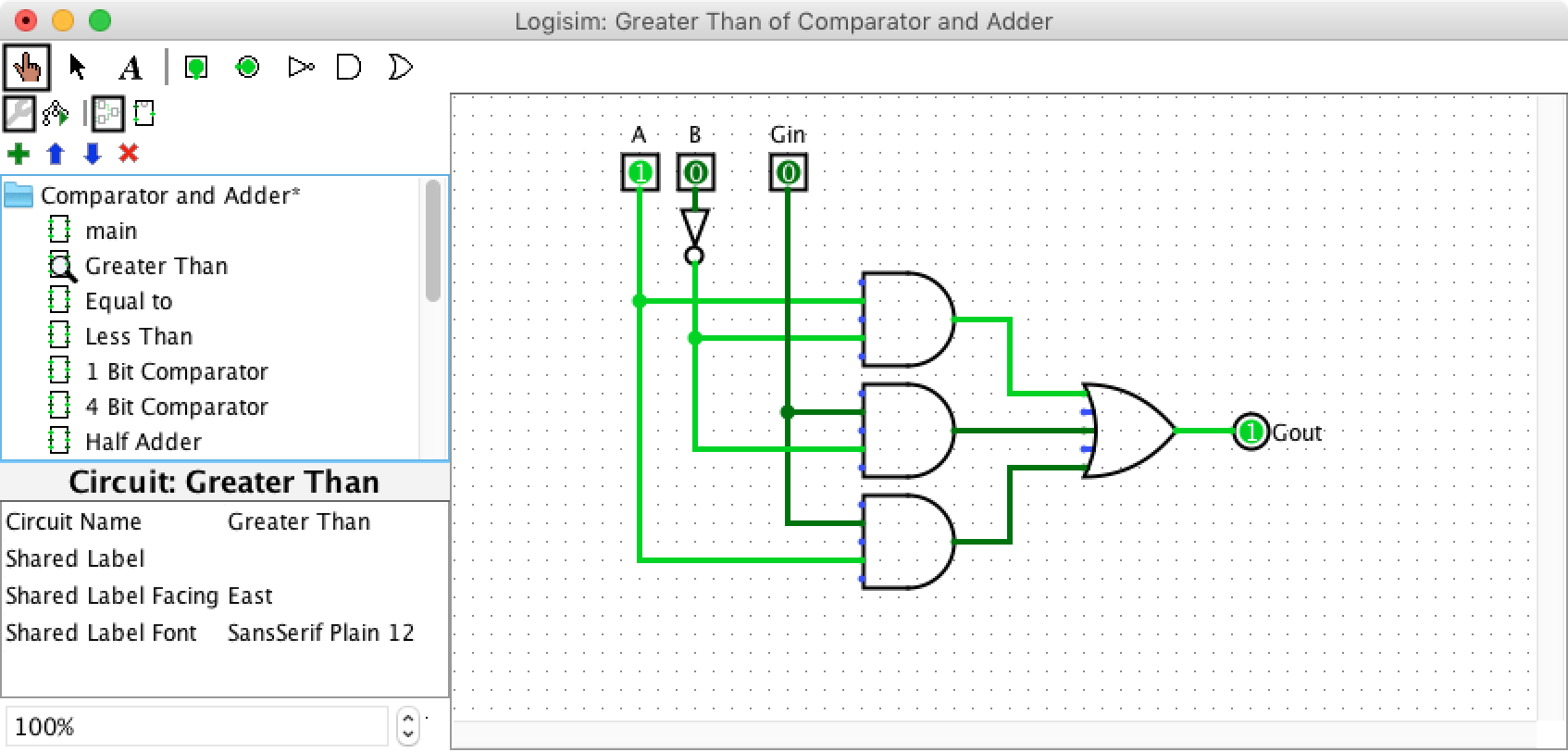
Starting off with something practical – it's often useful to be able to compare values, for example to check whether A is greater than B. A and B represent inputs and are one bit, so can be 0 or 1. The output should only be 1 if A is greater than B. This can be achieved with a single AND gate (the topmost of the three AND gates in the image), where the B input is inverted. For clarification, the third input Gin, along with the other two AND gates are used to allow multiple of these one-bit comparators to be connected in series to compare multi-bit numbers. And the OR gate in front of the output Goutsimply sets the output to 1 if any of the AND gates outputs a 1. I think you can image that “equal to” and “less than” are pretty similar.
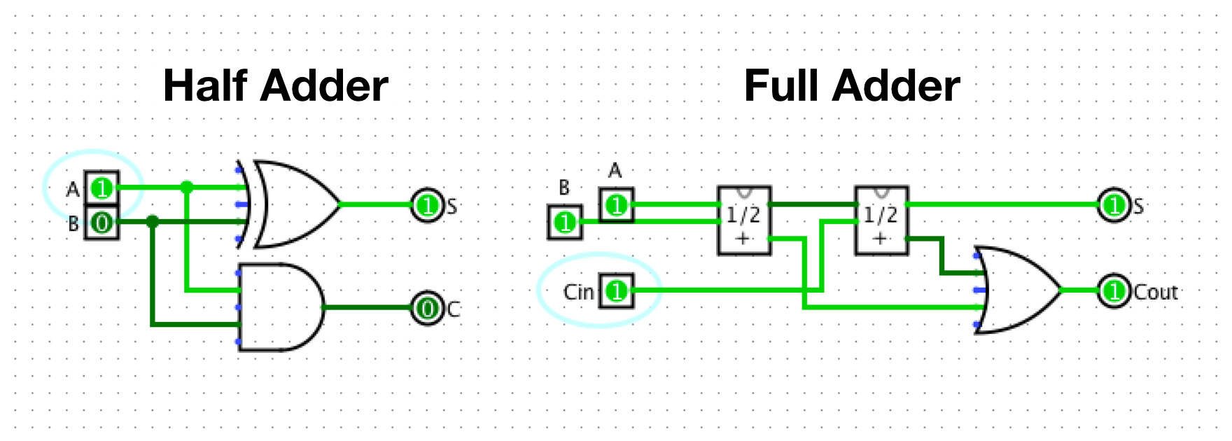
Perhaps another simple practical example – the addition of two values, achievable with a so-called “Half Adder”. If one of the inputs is a 1 and the other is a 0, the output should be 1, since 0+1=1. With both inputs 0 the output should be 0 and with both inputs 1 the carry flag C should be 1. With this description in mind, the main output is simply a XOR gate and the carry flag output is a simple AND gate. Furthermore, you can combine two Half Adders into a “Full Adder” with the ability to also handle a carry flag as input. For this reason, Full Adders can be connected in series to add larger numbers with many bits. These two examples are a part of what is happening in the ALU.
We also need a way to store some information. Apart from the RAM and ROM, there are a few places where we need to temporarily store some data in registers, e.g. the input numbers of the ALU or the Instruction Register IR, which stores the current instruction while it's being decoded and executed. Latches and Flip-Flops, which are Latches used in combination with a clock signal, are small circuits able to store some information. The simplest form, the “Set-Reset Latch”, will output a 1 after the Set S input is set to 1, and will remain 1 even when the S input is set to 0 again, thus storing the information. By setting the Reset R input to 1, it will output 0 again. Latches and Flip-Flops come in a few different flavors, and if you chain them together correctly, you get a Shift Register that can store multiple bits. The boxes on the right with the “D” their lower left corner are ”D Flip-Flops”. The key takeaway is that we have a bunch of inputs, and the shift register stores them when we give it the command. Afterwards, the inputs can change but the outputs will remain the previously defined values. A shift register has a few more tricks up its sleeve, it can shift the the stored data left or right, this would for example cause the state of Q0 being transferred to Q1 while the state of Q1 is transferred to Q2 and so on. Incidentally, this is useful, among other things, because the shifted number is equivalent to a number that is multiplied or divided by two.
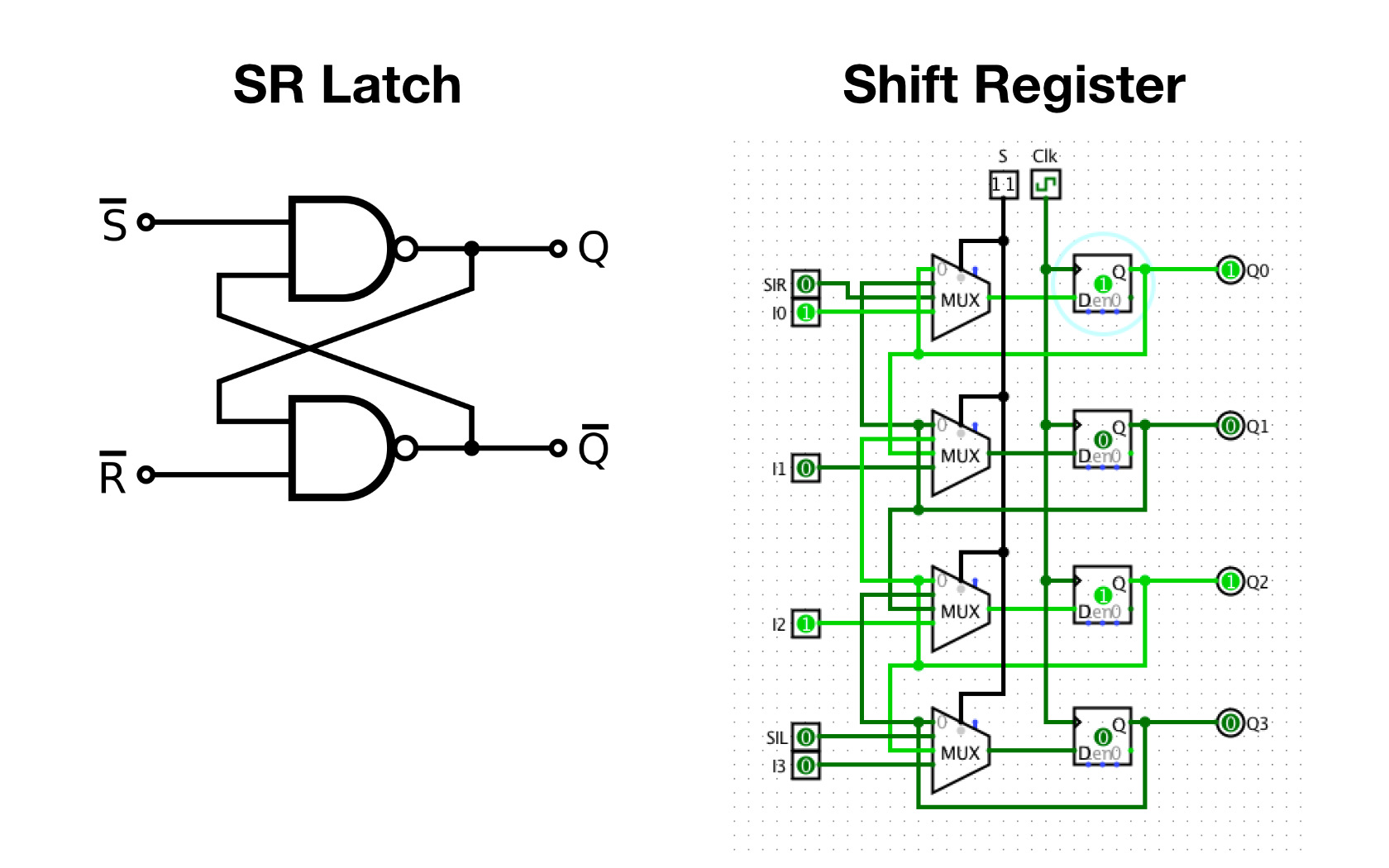
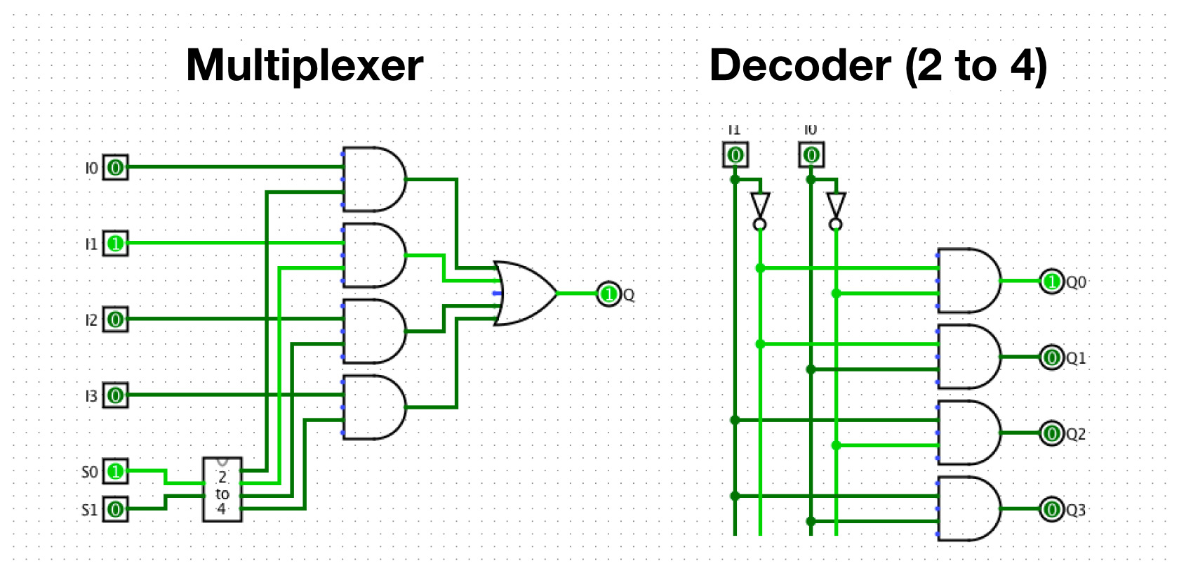
To realize these different functions of a Shift Register, the data entering the individual Flip-Flops must to be selectable. And this is achieved with the MUX parts. With a MUX or Multiplexer, we can use a few Select inputs (S0, S1) to choose which of the many inputs (I0, I1, I2, I3) to pass through the output Q. In theory, a MUX could have the same number of Select inputs and inputs to choose from. This would mean that if S0 (Select 0) was 1, the state of I0 (Input 0) would be reflected at the output. However, this leads to two problems: What if more than one Select input is 1 which Input should be selected? And secondly, it's a waste of inputs, since we can encode 4 states with only 2 inputs (00,01,10,11). To address both of these problems, we need a “Decoder”, basically a small circuit that converts binary input into a single output signal. So setting I0 to 0 and I1 to 1, which is the binary equivalent of the decimal number 2, causes Q2 to become 1. Both the Decoder and the Multiplexer are effectively just a number of AND gates, while the Multiplexer additionally combines them all with an OR gate to arrive at the single output we initially wanted. To finish the Shift Register story: A Shift Register also has Select Inputs to choose its mode of operation. When you choose a shift operation mode, the MUXs will select — depending on the chosen direction — the input that is connected to the Flip-Flop output on the right or left (that is, top or bottom in the image). This means that all the Flip-Flops will turn into their neighbors at the next Clock Clk signal. The clock signal basically tells the flip-flops to adopt the current input value now.
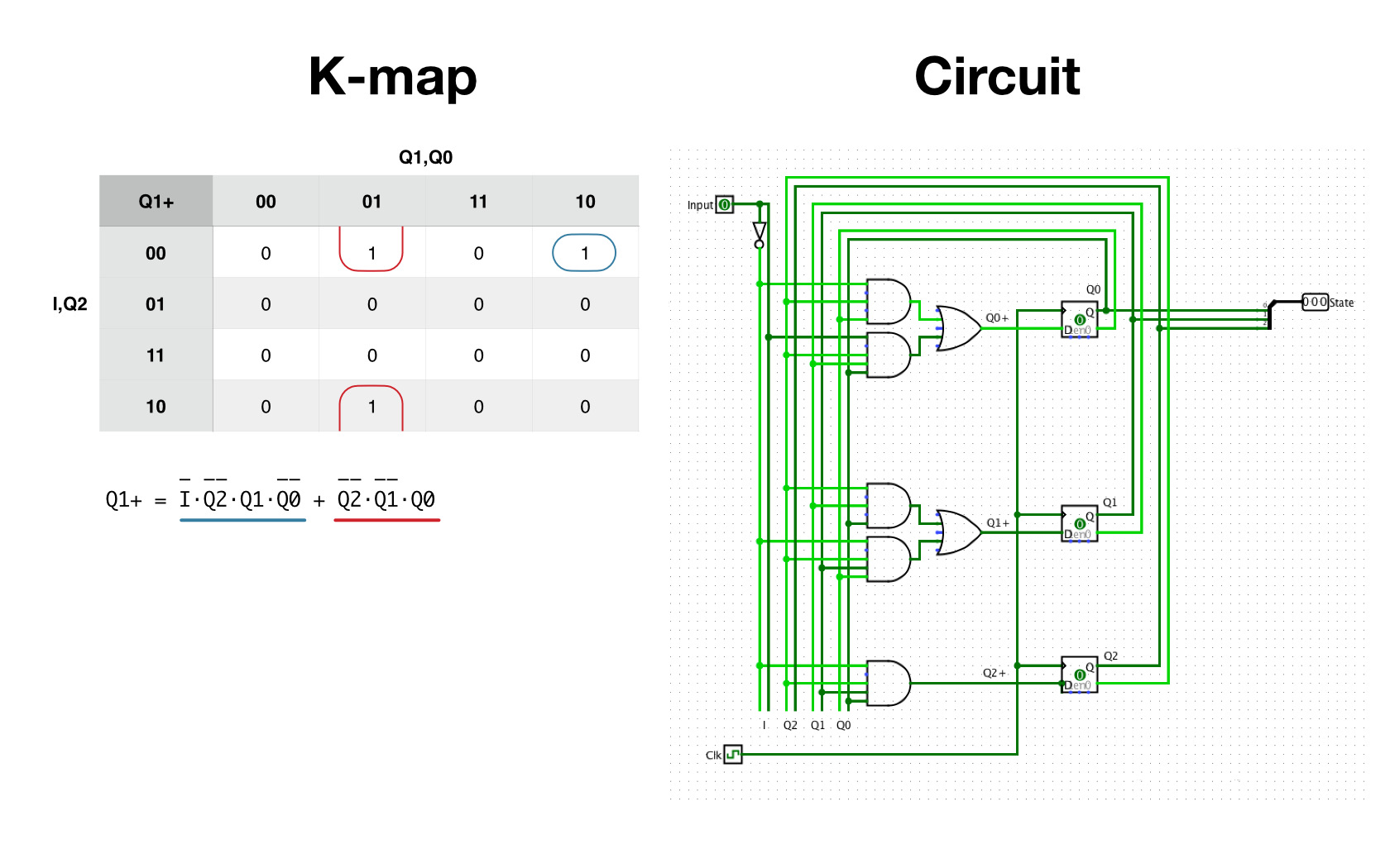
I think you slowly get the idea that it's all “just” a bunch of inputs and outputs. Now, if we want to have a certain functionality from all these different parts, we need to set a specific set of inputs to 1. And this is where the Control Unit CU comes into play. Based only on the state of the state machine and the current instruction, it manages all the parts so that they play neatly together to achieve the desired result. To fully execute an instruction from ROM, several steps must be performed in the correct order, and this is where a finite state machine FSM shines (CU FSM in the overview image). It's basically a description of several states, and how to get from one state to another. Thereby only one state can ever be active. In this case, the states are “Fetch Instruction”, “Decode Instruction”, “Process Operands” and “Execute”. The state machine has a single input that decides whether one or the other transition occurs. It also encodes the states S0 through S4 with with output bits Q0, Q1 and Q2. These output bits are also used as inputs to help with the decision of which state should come next, represented by Q0+, Q1+ and Q2+. It's a fairly simple state machine, as long as the Input I is 0, one state is followed by the next, if Input I is 1, it returns to the initial S0 state, with the exception of S1. Here we want to skip S2 when Input I is 1. This is useful because it skips the processing of one of the two possible operands for instructions that use only one operand. Converting the state diagram into a truth table is pretty straightforward.

To build the logic for this state machine, you could look at the 1s for each output. For each individual 1, you could feed the necessary conditions for all four inputs into an AND gate, and finally combine all of those AND outputs with an OR gate, which represents the final result for that output. This would certainly work, but there is a better way to save a few logic gates, although I have to say there are better examples to illustrate that point, but we'll work with what we have. We start similarly, by looking at each output, let's choose Q1+. In principle, we transform the truth table above into a different form called Karnaugh map or “K-map”. The advantage of this table is its visualization, it helps us to visually group 1s together that form a rectangle. It should be noted that the edges of the table wrap around. The more 1s we are able to group together, the simpler the resulting Boolean Expression will be. Most of the 1s in this state machine are “on their own”, without many grouping opportunities. For a 1 that is not groupable, like the one in the upper right corner, we have to use all four inputs to define that output (as we did in the initial approach). However, for groupable 1s, we have the opportunity to simplify the expression by removing the inputs for which it does not matter whether they are a 0 or a 1. Here in the second column we can simplify by removing the I Input. This way we don't need two AND gates with four inputs each, but only one AND gate with only three inputs for the two 1s – quite an improvement. As with the gates, there are different symbols used around the world for the logic expressions. Here, the + signifies a OR and a ⋅ (which could be omitted) represents a logical AND. The overline indicates that this symbol is inverted, meaning a 0 is necessary. From this expression we can build the final circuit you can see on the right.
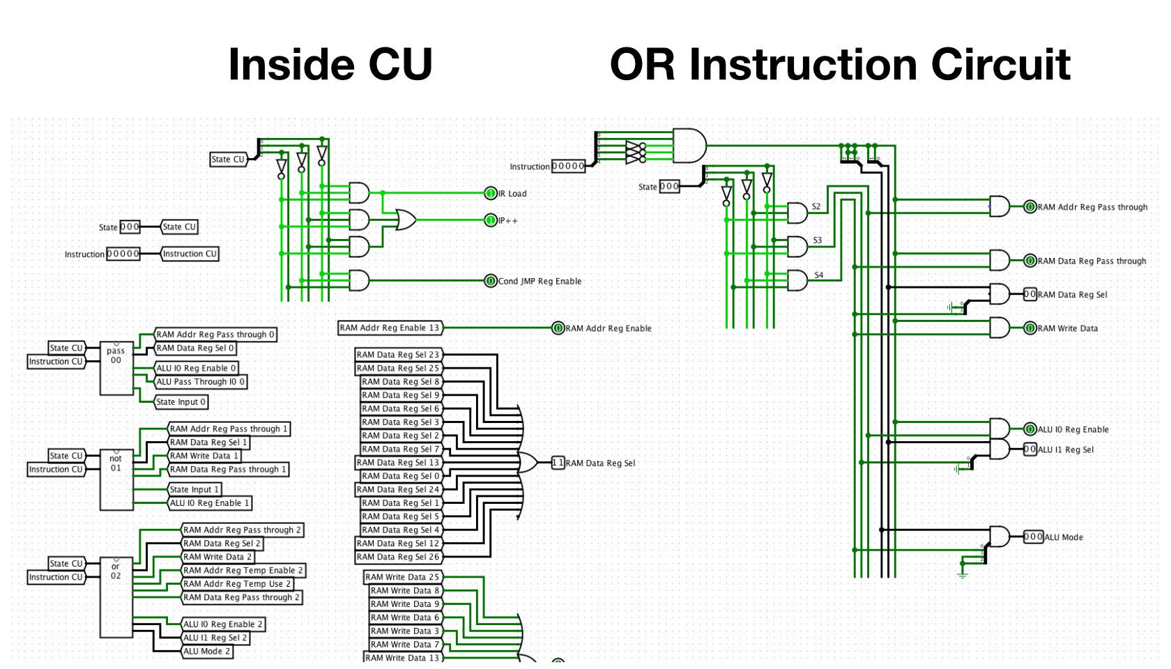
By using a “Clock” Clk we can move the state machine forward one step with each tick. Inside the Control Unit box there are many smaller circuits that control its outputs for each individual instruction. These instruction circuits are only “activated” when the corresponding instruction has been decoded. And that is basically how we can tell the CPU what to do by entering an instruction opcode into the ROM where it can be fetched, decoded and executed by the Control Unit.
And coming full circle, we are back to the initial overview image. If you look closely at the Output register, you can see how the binary equivalents of the first few Fibonacci Numbers (0, 1, 1, 2, 3, 5, 8) are displayed. Like I mentioned earlier, real modern CPUs are much more complex and not everything we've learned here can be applied 1 to 1 to them, and yet I've barely scratched the surface of this design. But I hope this post has given a tiny helpful insight to make computers a little less mysterious.
The source code and instruction on how to use this project can be found on this GitHub page.